Nanotechnology: Engineering the World at the Atomic Scale
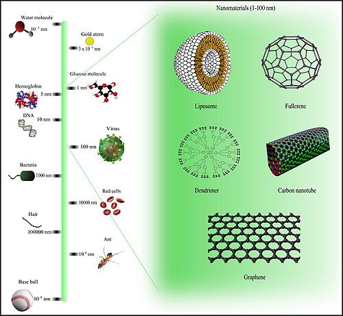
Nanotechnology is the manipulation of matter on an incredibly small scale, specifically where at least one dimension is sized from 1 to 100 nanometers (nm). To put this in perspective, a nanometer is one-billionth of a meter. At this nanoscale, the traditional laws of physics shift; surface area increases dramatically and quantum mechanical effects begin to dominate, fundamentally altering how matter behaves.
While the terms are often used interchangeably, a distinction exists between nanoscience and nanotechnology. Nanoscience focuses on the pure scientific study of these phenomena—including nanophysics, nanochemistry, and nanobiology. Nanotechnology, conversely, represents the applied side, utilizing these scientific insights to create concrete methods and processes, such as nanolithography and nanobiosensing, for use in nanoengineering and nanomedicine.
Key Facts
- Scale: Operates within the 1 to 100 nanometer range.
- Core Driver: Properties change at this scale due to quantum effects and increased surface-area-to-volume ratios.
- Interdisciplinary Nature: Integrates surface science, organic chemistry, molecular biology, and semiconductor physics.
- Primary Methods: Employs both "top-down" (carving) and "bottom-up" (assembling) fabrication techniques.
- Key Materials: Includes carbon-based structures like fullerenes and nanotubes, as well as metallic nanowires.
The Spectrum of Nanoscale Science
Nanotechnology is not a single field but an umbrella for various research areas. It ranges from extending conventional device physics to the direct control of individual atoms. One specialized branch, molecular nanotechnology, focuses on the precise manipulation of atoms and molecules to fabricate macroscale products.
From Simple to Complex Structures
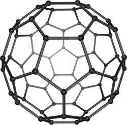
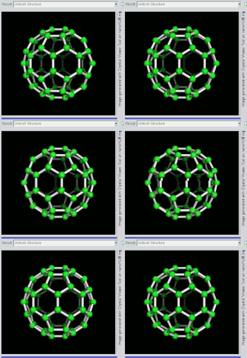
At the molecular level, researchers work with structures like fullerenes. A prime example is Buckminsterfullerene (C60), often called the "buckyball," which serves as a representative member of the fullerene family.
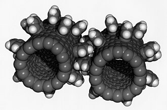
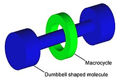
Beyond simple spheres, scientists have developed more complex molecular machines. These include rotaxanes, which can function as molecular switches, and fullerene nanogears that mimic mechanical movement at a microscopic level.
Biological Nanostructures
Nature is the original nanotechnologist. The ribosome, for instance, acts as a biological molecular assembler by translating DNA into proteins. Modern science mimics this through DNA nanotechnology, creating artificial structures like DNA tetrahedrons, where each edge is a 20 base pair double helix.

![This DNA tetrahedron[42] is an artificially designed nanostructure of the type made in the field of DNA nanotechnology. Each edge of the tetrahedron is a 20 base pair DNA double helix, and each vertex is a three-arm junction.](/images/b6/91/b691642206440d7adb1944c2ba0e0646ee74dfb85b60b8d3c32b8221140cb6b3.png)
Fabrication Approaches and Tools
Creating materials at the nanoscale requires specialized strategies, generally categorized into two primary philosophies: top-down and bottom-up.
Top-Down vs. Bottom-Up
- Top-Down Approach: This involves starting with a larger piece of material and removing parts to create a smaller structure, similar to sculpting. An example is nanolithography, used extensively in semiconductor manufacturing.
- Bottom-Up Approach: This method builds structures atom-by-atom or molecule-by-molecule. A key concept here is molecular self-assembly, where molecules spontaneously organize into structured patterns.
Precision Tools for Visualization
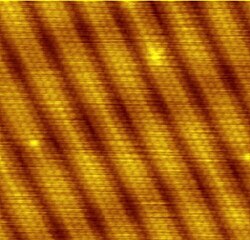
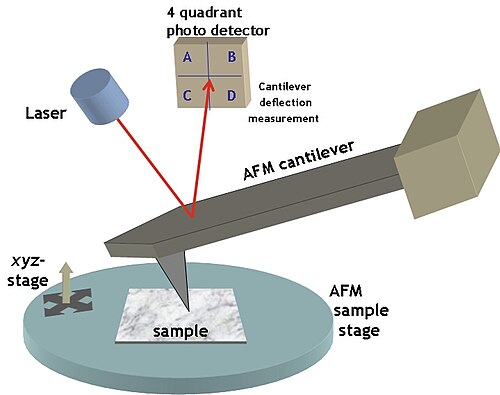
Because nanostructures are too small to be seen with visible light, scientists use scanning microscopes. The Scanning Tunneling Microscope (STM) can visualize individual atoms on a surface, such as a clean Gold(100) surface. Similarly, the Atomic Force Microscope (AFM) uses a microfabricated cantilever with a sharp tip to "feel" the surface of a sample, translating deflections into a detailed image.
Modern Applications of Nanotechnology
The practical application of these technologies is already transforming several industries, from energy to electronics.
Nanoelectronics and Photonics
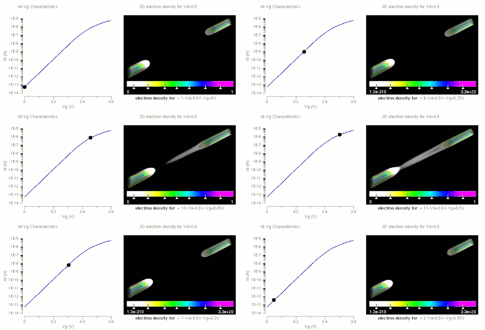
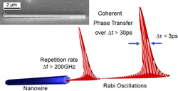
In the realm of electronics, MOSFETs (Metal-Oxide-Semiconductor Field-Effect Transistors) are being developed using nanowires approximately 10 nm in length. Furthermore, nanowire lasers are being utilized for the ultrafast transmission of information via light pulses.
Energy and Light
Nanoscale materials, such as nanopillars, are integrated into solar cells to improve efficiency. Other devices utilize quantum wells to transfer energy to nanocrystals, which then emit visible light.
![This device transfers energy from nano-thin layers of quantum wells to nanocrystals above them, causing the nanocrystals to emit visible light.[43]](/images/35/a6/35a6d32e74a85d2ad928fe9b22b7f649c3caa38b807f398fc563cdaff29190d9.jpg)
| Category | Key Example/Tool | Primary Function/Purpose |
|---|---|---|
| Carbon Nanostructures | C60 (Buckyball) | Fundamental research in fullerenes |
| Imaging Tools | AFM / STM | Visualizing and manipulating atoms |
| Fabrication | Self-assembly | Bottom-up construction of materials |
| Electronics | Nanowire MOSFETs | Miniaturization of computing components |
| Biotechnology | DNA Tetrahedron | Artificial nanostructure design |
Safety, Health, and Regulation
The unique properties of nanomaterials also introduce new risks. There are ongoing concerns regarding the toxicity of nanoparticles and how they interact with biological systems. For example, research has investigated whether inhaled nanoparticles can travel from the nose to the brain or if certain nanotubes could potentially lead to cancer.
Due to these uncertainties, the field is subject to evolving regulation. Discussions center on whether the industry should move toward self-regulation with limited oversight or implement stricter government-mandated safety guidelines to protect workers and the environment.
Frequently Asked Questions
What is the difference between nanoscience and nanotechnology?
Nanoscience is the study of the fundamental properties of matter at the nanoscale, while nanotechnology is the application of that science to create products, devices, and processes.
What is a "bottom-up" approach in nanotechnology?
A bottom-up approach is a fabrication method where complex structures are built from the ground up, starting with individual atoms or molecules, often utilizing molecular self-assembly.
What are fullerenes?
Fullerenes are a family of carbon structures, the most famous of which is the C60 buckyball, a spherical molecule composed of 60 carbon atoms.
Why do materials behave differently at the nanoscale?
At the nanoscale, the ratio of surface area to volume increases significantly, and quantum mechanical effects become dominant, changing the chemical, electrical, and physical properties of the material.
Are there health risks associated with nanotechnology?
Yes, there are concerns that certain nanoparticles may be toxic or capable of penetrating biological barriers (like the blood-brain barrier) in ways that larger particles cannot, leading to ongoing safety and regulatory research.