ggNMOS ESD Protection in CMOS Integrated Circuits
In the world of semiconductor manufacturing, ensuring the longevity and reliability of a chip is a constant challenge. One of the most significant threats to integrated circuits (ICs) is electrostatic discharge (ESD)—the sudden flow of electricity between two electrically charged objects. To combat this, engineers utilize specialized components like the Grounded-gate NMOS, or ggNMOS, to shield sensitive internal components from catastrophic failure.
What is ggNMOS?
A ggNMOS is a specific type of electrostatic discharge protection device integrated into CMOS (Complementary Metal-Oxide-Semiconductor) circuits. Its primary purpose is to safeguard the input and output (I/O) pins of an IC. These pins are particularly vulnerable because they are accessed off-chip, either through wire-bonding to package pins or via direct connections to a printed circuit board (PCB), making them the first point of contact for external electrical surges.
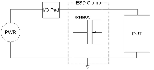
How ESD Protection Works
When an ESD event occurs, a massive amount of energy is delivered to the chip in a very short window of time. Without protection, this energy would surge through the delicate I/O circuitry, likely destroying the device. The ggNMOS device acts as a safety valve; it provides a low-resistance, safe path for the current to flow away from the sensitive internal logic and toward the ground.
This mechanism is critical for maintaining product reliability. Statistics indicate that 35% of all IC failures encountered in the field are directly associated with ESD damage, highlighting the necessity of robust protection schemes.
Key Facts
- Function: Provides a safe current path to prevent ESD energy from destroying sensitive I/O circuitry.
- Application: Used in CMOS integrated circuits to protect off-chip access points.
- Impact: ESD damage accounts for 35% of all IC failures in the field.
- Placement: Positioned at inputs and outputs that are wire-bonded or connected to PCBs.
Summary of ESD Protection Impact
| Factor | Detail |
|---|---|
| Primary Threat | Electrostatic Discharge (ESD) |
| Protection Device | ggNMOS (Grounded-gate NMOS) |
| Vulnerable Areas | Off-chip I/O pins and PCB connections |
| Failure Rate | 35% of field failures linked to ESD |
Frequently Asked Questions
What does ggNMOS stand for?
ggNMOS stands for Grounded-gate NMOS, a specific configuration of an N-channel MOSFET used for electrostatic discharge protection.
Why are I/O pins more susceptible to ESD?
I/O pins are the points where the chip connects to the outside world via wire-bonds or PCBs, making them the most likely entry points for external electrical charges.
How does a ggNMOS device prevent chip failure?
It diverts the high-energy current from an ESD event away from sensitive internal circuitry and provides a safe path for that current to dissipate.
How common is ESD damage in the field?
ESD damage is quite prevalent, contributing to approximately 35% of all integrated circuit failures once they are deployed in the field.
In what type of circuits is ggNMOS typically used?
It is commonly used within CMOS (Complementary Metal-Oxide-Semiconductor) integrated circuits.